- 您现在的位置:买卖IC网 > Sheet目录996 > NCP5602EVB (ON Semiconductor)EVAL BOARD FOR NCP5602
�� �
�
�NCP5602�
�APPLICATION� INFORMATION�
�DC� ?� DC� Operation�
�The� converter� is� based� on� a� charge� pump� technique� to�
�generate� a� DC� voltage� capable� to� supply� the� White� LED�
�load.� The� system� regulates� the� current� flowing� into� each�
�LED� by� means� of� internal� current� mirrors� associated� with�
�the� white� diodes.� Consequently,� the� output� voltage� will� be�
�equal� to� the� Vf� of� the� LED,� plus� the� drop� voltage� (ranging�
�from� 200� mV� to� 400� mV,� depending� upon� the� output�
�current)� developed� across� the� internal� NMOS� mirror.�
�Typically,� assuming� a� standard� white� LED� forward� biased�
�at� 10� mA,� the� output� voltage� will� be� 3.8� V.�
�The� built� ?� in� OVP� circuit� continuously� monitor� each�
�output� and� stops� the� converter� when� the� voltage� is� above�
�Rbias� +� 300� Iout� (eq.� 2)�
�Consequently,� the� resistor� value� will� range� between�
�R� bias� =� 300/30� mA� =� 10� k� W� and� R� bias� =� 300/0.5� mA� =�
�600� k� W� .� Obviously,� the� tolerance� of� such� a� resistor� must� be�
�1%� or� better,� with� a� 100� ppm� thermal� coefficient,� to� get� the�
�expected� overall� tolerance.�
�VBandgap�
�5.0� V.� The� converter� resumes� to� normal� operation� when� the�
�voltage� drops� below� 5.0� V� (no� latchup� mechanism).�
�Consequently,� the� chip� can� operate� with� no� load� during� any�
�test� procedures.�
�Load� Current� Calculation�
�I� REF�
�+�
�-�
�600mV�
�LED� Return�
�Pin� 2� &� 3�
�The� load� current� is� derived� from� the� 600� mV� reference�
�voltage� provided� by� the� internal� Bandgap� associated� to� the�
�external� resistor� connected� across� I� REF� pin� and� Ground� (see�
�Figure� 3).� In� any� case,� no� voltage� shall� be� forced� at� I� REF�
�pin,� either� downward� or� upward.�
�The� reference� current� is� multiplied� by� the� constant�
�R1�
�GND�
�Pin� 4�
�GND�
�Note:� The� I� REF� pin� must� never� be�
�biased� by� an� external� voltage.�
�Figure� 3.� Basic� Reference� Current� Source�
�Rbias� +� (Vref� *� k)� Iout�
�k� =� 500� to� yield� the� output� load� current.� Since� the� reference�
�voltage� is� based� on� a� temperature� compensated� Bandgap,�
�a� tight� tolerance� resistor� will� provide� a� very� accurate� load�
�current.� The� resistor� is� calculated� from� the� Ohm’s� law�
�(R� bias� =� Vref/I� REF� )� and� a� more� practical� equation� can� be�
�arranged� to� define� the� resistor� value� for� a� given� output�
�current:�
�(eq.� 1)�
�Rbias� +� (0.6� *� 500)� Iout�
�7�
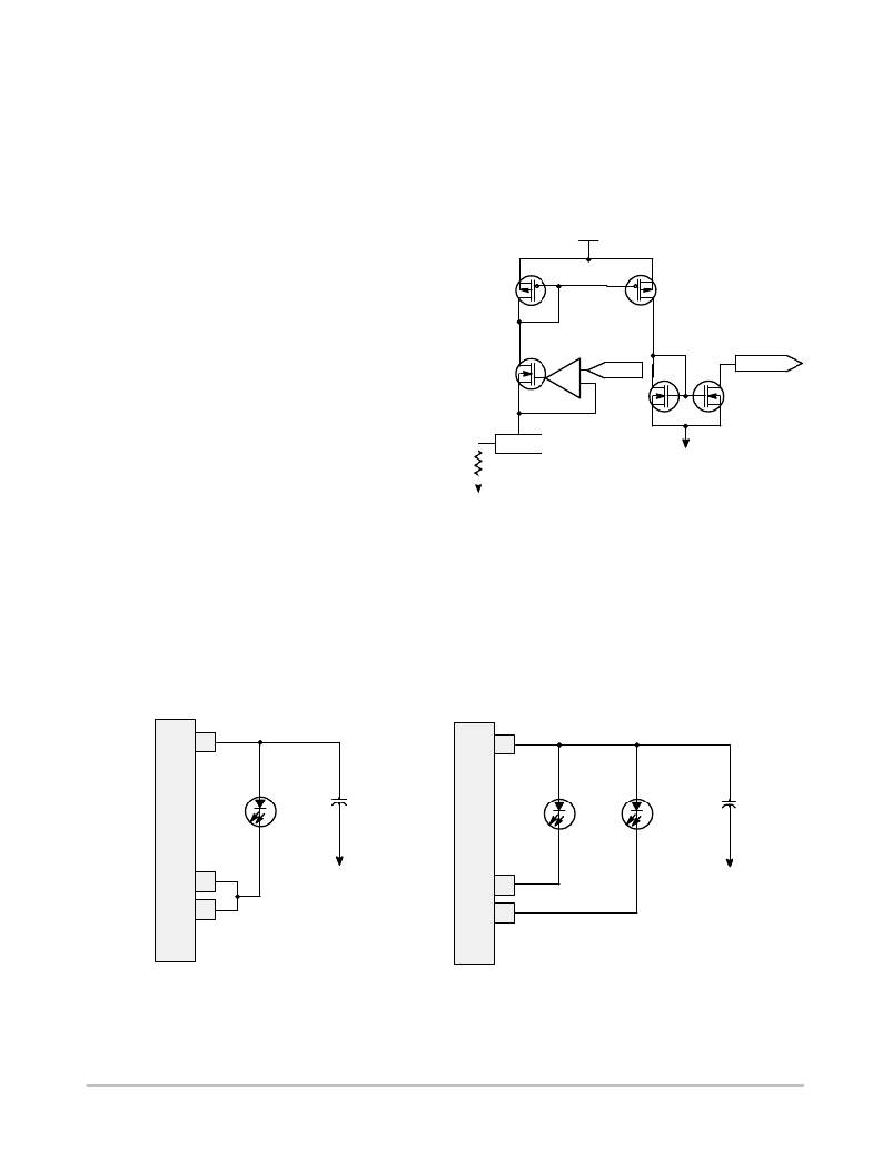
�Load� Connection�
�The� NCP5602� chip� is� capable� to� drive� the� two� LED�
�simultaneously,� as� depicted� in� Figure� 1,� but� the� load� can� be�
�arranged� to� accommodate� one� or� two� LED� if� necessary� in�
�the� application� (see� Figure� 4).� In� this� case,� the� two� current�
�mirrors� can� be� connected� in� parallel� to� drive� a� single� power�
�full� LED,� thus� yielding� 60� mA� current� capability� in� a� single�
�LED.�
�7�
�2�
�3�
�GND�
�2�
�3�
�GND�
�Figure� 4.� Typical� Single� and� Double� LED� Connections�
�http://onsemi.com�
�6�
�发布紧急采购,3分钟左右您将得到回复。
相关PDF资料
NCP5603GEVB
EVAL BOARD FOR NCP5603G HI FREQ
NCP5604AAGEVB
EVAL BOARD FOR NCP5604AAG
NCP5608EVB
EVAL BOARD FOR NCP5608
NCP5612GEVB
EVAL BOARD FOR NCP5612G
NCV7680PWR22GEVB
BOARD EVALUATION NCV7680
NDNA200
DIN-RAIL 35MM ALUMINUM 2M
NG-9517
CABLE GLAND NEMA 4X PG-29 BLACK
NH2503K000FJ01
250WATTS 3KOHMS 1% NON-INDUCTIVE
相关代理商/技术参数
NCP5602MUTBG
功能描述:LED照明驱动器 WHITE LED DRIVER- 2LED-I2C RoHS:否 制造商:STMicroelectronics 输入电压:11.5 V to 23 V 工作频率: 最大电源电流:1.7 mA 输出电流: 最大工作温度: 安装风格:SMD/SMT 封装 / 箱体:SO-16N
NCP5603
制造商:ONSEMI 制造商全称:ON Semiconductor 功能描述:AC-DC Offline Switching Controllers/Regulators
NCP5603GEVB
功能描述:LED 照明开发工具 NCP5603 EVAL BRD
RoHS:否 制造商:Fairchild Semiconductor 产品:Evaluation Kits 用于:FL7732 核心: 电源电压:120V 系列: 封装:
NCP5603MNR2
功能描述:LED照明驱动器 4.5V/5.0V Hi Eff. RoHS:否 制造商:STMicroelectronics 输入电压:11.5 V to 23 V 工作频率: 最大电源电流:1.7 mA 输出电流: 最大工作温度: 安装风格:SMD/SMT 封装 / 箱体:SO-16N
NCP5603MNR2G
功能描述:LED照明驱动器 4.5V/5.0V Hi Eff. White LED Driver RoHS:否 制造商:STMicroelectronics 输入电压:11.5 V to 23 V 工作频率: 最大电源电流:1.7 mA 输出电流: 最大工作温度: 安装风格:SMD/SMT 封装 / 箱体:SO-16N
NCP5603MNR2G-CUT TAPE
制造商:ON 功能描述:NCP5603 Series 200 mA 5.5 V SMT High Efficiency Charge Pump Converter - DFN-10
NCP5604A
制造商:ONSEMI 制造商全称:ON Semiconductor 功能描述:High Efficiency White LED Driver
NCP5604AAGEVB
功能描述:电源管理IC开发工具 NCP5604 EVAL BRD
RoHS:否 制造商:Maxim Integrated 产品:Evaluation Kits 类型:Battery Management 工具用于评估:MAX17710GB 输入电压: 输出电压:1.8 V